Get a turnkey engineering service for semiconductor tools that you can rely on
For more than 30 years, we’ve been working with complex semiconductor tools (from implanters to lithography) in fabs all over the world. Our turnkey service covers every step of your semiconductor relocation, start-up and commission.
Start-to-finish relocation partner for production-critical tools
We work with IES because we trust them. We know that when a critical situation occurs and we have a tool down they’ll support us, not just with parts but also by providing experienced engineers if we need them. It’s a complete solution."
Implant Centre Manager,
Analog Devices
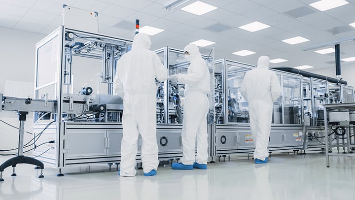
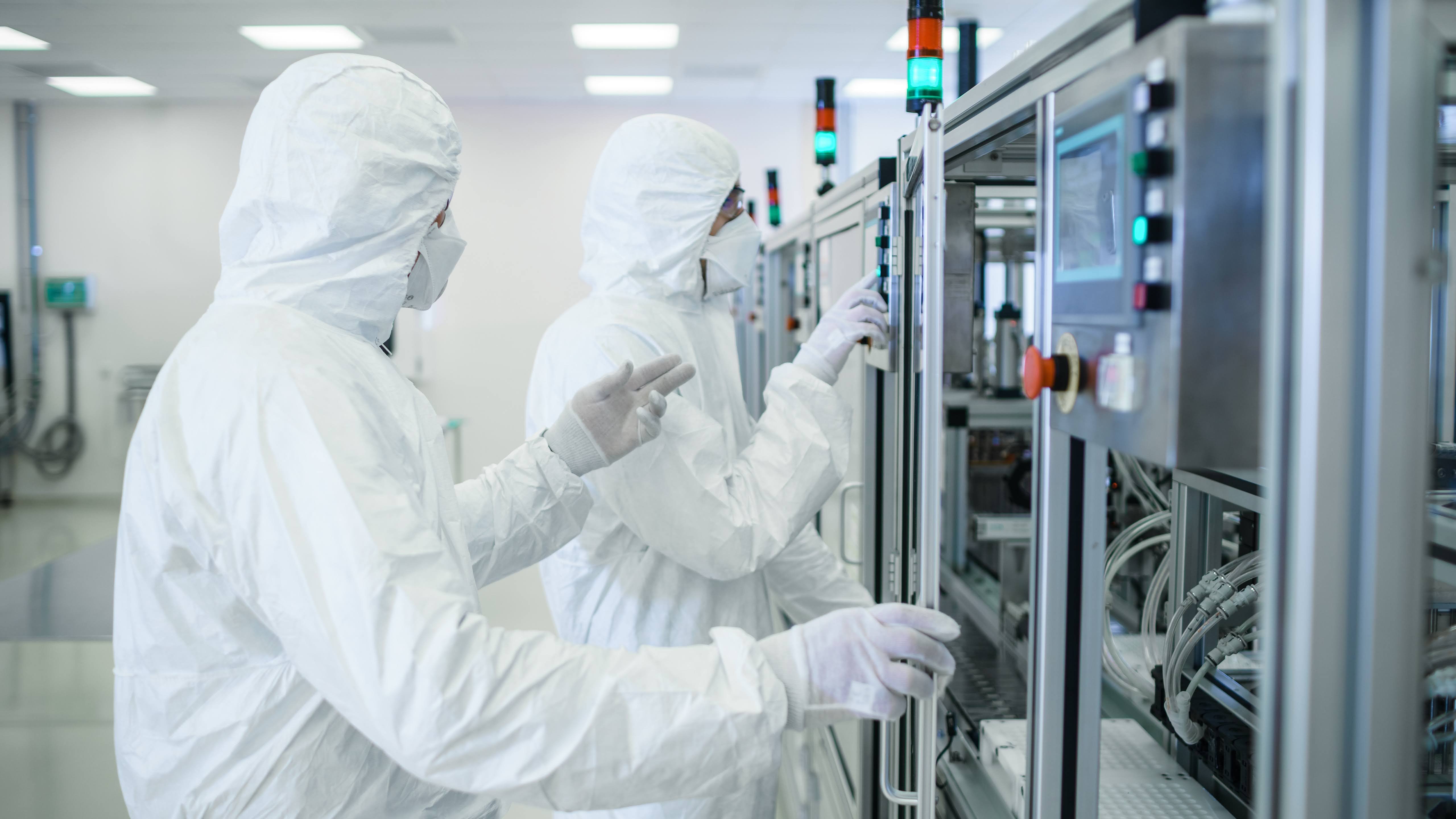
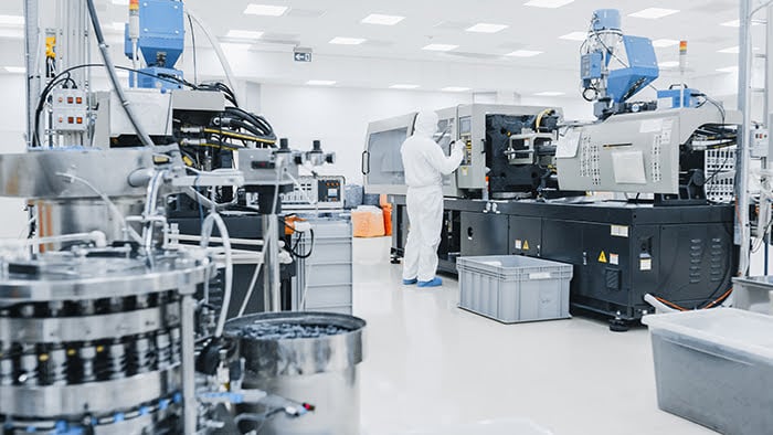
What we do
From single tool start-ups to complete production line relocations, decontamination and modifications; IES is the trusted provider of engineering services to the semiconductor sector. Benefit from a start-to-finish service:
Comprehensive site surveys, method statements and risk assessments
Decontamination
Tool dismantling and de-installation
Shipping brackets/lockdown kit
Tool move-out
Export packing
Door-to-door freighting, including customs
Tool move-in
Assembly and start-up
Final tests
Additional support services
Pedestal floors
Upgrades
Compliance testing - including UKCA/CE and PUWER assessments
Trusted by Microchip, Analog Devices, Nexperia and more
We've supported both manufacturers and end users to move, install and commission semiconductor tools since 1991, and have strong working relationships with many world-class microelectronics manufacturers.
We helped Plessey Semiconductors move more than 90 semiconductor tools into its new facility in 18 months.
“IES are reliable, flexible, and knowledgeable of the semiconductor industry, so were the best partner for the installation project.” - Chief Operating Officer, Plessey Semiconductors