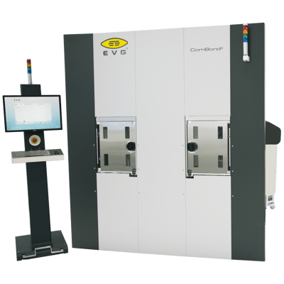
ComBond
The EVG ComBond platform directly addresses market demand for a higher level of sophistication in integration processes. It is a high-vacuum wafer bonding platform which is considered a flagship system in EVG’s unique wafer bonding technology and equipment portfolio.
With its modular cluster design, the EVG ComBond supports application areas including stacked solar cells, advanced engineering substrates, high end MEMS packaging, power devices, ‘beyond CMOS’ devices, and high performance logic. The EVG ComBond’s flexibility means it can be adapted to several challenging customer requirements in both high-throughput manufacturing environments, and R&D settings.
The platform enables the bonding of coefficients of thermal expansion (CTE) and various lattice constants with heterogeneous materials, along with the creation of bond interfaces which are electrically conductive; it does this via a unique oxide removal process. Thanks to the high vacuum technology offered by the EVG ComBond, the low temperature bonding of metals is possible, with re-oxidising occurring rapidly in ambient environments. Superior bond strength and particle, and void-free interfaces, can be attained with all material combinations.
Features
- High-vacuum, aligned, covalent bonding
- Processing in high-vacuum environment (< 5·10-8 mbar)
- In-situ sub-micron face-to-face alignment accuracy
- High-vacuum MEMS and optical device encapsulation In-situ surface and native oxide removal
- Superior surface properties
- Conductive bonding
- Room-temperature process
- Multiple material combinations, including metals (aluminum)
- Stress-free bond interface
- High bond strength
- Modular system for HVM and R&D
- Flexible configurations up to six modules
- Substrate size up to 200 mm
- Fully automated


